The Consortium Approach. Strategic Goals, Vision and Mission
The integrated circuitry (IC) industry is entering an innovation and manufacturing world where Moore’s law ran out of steam and is being replaced by heterogeneous integration of systems in package (SIPs) for high performance computing (HPC). As a result, the IC industry is facing a convergence of ever more intricate technological obstacles and taxing financial constraints. Research and development (R&D) and manufacturing capital costs are continuing to rise at an exponential rate, a trend that is already placing tremendous strain on the fiscal integrity and business competitiveness of even the largest global semiconductor corporations. According to the analysis by McKinsey & Company, and as shown in Exhibit I, the cost of computer chip design has soared from $28 million for the 65nm node to $540 million for the 5nm node. Similarly, the corresponding price tag for fab (as in computer chip fabrication plant) construction has burgeoned from $400 million for the 65nm node to over $5 billion for the 5nm node.
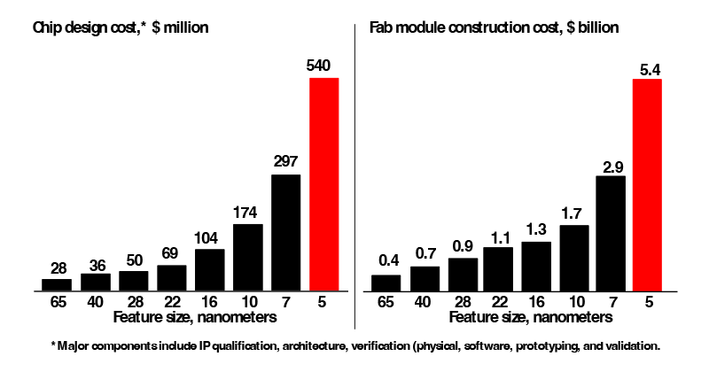
Exhibit I. Computer chip R&D and manufacturing expenses continue to soar with the introduction of every new generation (source: McKinsey & Company).
The findings of the McKinsey & Company report were echoed by Handel Jones, CEO of International Business Strategy Corporation (IBS), who stated: "The average cost of designing a 28nm chip is US$40 million. By comparison, the cost of designing a 7nm chip is US$217 million and the cost of designing a 5nm device is US$416 million. 3nm design will cost up to 590 million US dollars."
These costs do not include expenditures associated with prototyping and demonstration of chip fabrication processes. According to Semiconductor Engineering, a widely recognized semiconductor research association, the investment in processes for the 28nm node averaged around $51.3 million. This number increased to $100 million, $297 million, and $542 million for the 16nm, 7nm, and 3nm nodes, respectively. And although the data for the 3nm node is not yet completely accessible, most likely since it remains in the development and optimization phase, Semiconductor Engineering estimates the cost to very easily exceed $1 billion. In fact, IBS predicts that the 3nm node process development and demonstration will require US$4-$5 billion, and the corresponding FAB construction and outfitting cost will average US$15-20 billion. In fact, both TSMC and Intel have announced up to US$20 billion investment each in their first 3nm FABs.
The ramifications of this trend become obvious when MacKenzie & Company examined the operations of the two main groups of semiconductor companies, namely, the leading chain of chip manufacturers and the support chain of ancillary industrial companies (chemical and materials producers, component suppliers, OEMs, packaging and testing concerns), the latter is by far the most negatively impacted by the exponential cost increase. This adverse impact has significant and long-term implications for the entire U.S. (and New York) semiconductor industry which relies on this worldwide vendor’s value chain to provide all its chemicals, equipment, components, materials, consumables, and supplies. It has also led to a recent and ongoing flurry of company acquisitions and corporate mergers across the entire semiconductor supply chain. As a result, the semiconductor supply chain has been reduced to clusters of vendors that are mainly located outside the U.S. (primarily the Pacific rim) and that dominate the market for specific goods and services to the entire industry.
From an economic perspective, this consolidation of the industrial vendor's chain leaves the U.S. computer chip producers vulnerable to supply-chain disruptions. These disruptions could be compounded by political upheavals, geopolitical tensions, military conflicts, pandemics, and natural disasters, as seen in the Covid-19 shutdown and the Ukrainian-Russian war. As a result, the McKinsey & Company report warns that “…If a key vendor cannot ship products or meet delivery deadlines, production lines could grind to a halt. More widespread upheaval, such as the global lockdowns in response to the COVID-19 pandemic, have even greater repercussions…” The McKinsey & Company report goes on to argue that “…to accommodate unexpected shortages, companies need flexible and resilient supply chains that can quickly adjust…”
Accordingly, these global disruptions have accentuated the necessity for a reliable and dependable U.S.-based vendor resource, one that would not only supply current domestic industry needs, but also contribute innovations that would shield the U.S. semiconductor industry from future liabilities related to dependence on foreign suppliers, particularly outfits that could be averse to US interests. In fact, with the move towards heterogeneous integration systems in package (SIPs) for high performance computing (HPC), innovations in chemistry and materials are replacing design and architecture as the most critical enabler of computer chip advancement. Chemical and material suppliers are therefore playing a leadership position in the innovation and discovery loop. This represents an excellent opportunity to reclaim and re-shore the IC value supply chain to the U.S. Failure to exploit this inflection opportunity to onshore and secure chemical and material supply chain in the USA, would not only threaten its leading position in technology and defense capability, but it may also cause a permanent off shoring of R&D and manufacturing of the entire semiconductor supply chain.
It is therefore imperative to establish a reliable and dependable U.S.-based chemical and material vendor supply consortium, one that would support the strategic interests and economic competitiveness of the U.S. Federal government, individual states, as well as American computer chip corporations, in IC innovation and manufacturing. To this end, of the $39 billion in subsidies for chip manufacturing authorized under the Chips and Science act, which was enacted by the 117th United States Congress and signed into law by President Joe Biden on August 9, 2022, over $30 billion has so far been awarded to the leading chain of chip manufacturers to build their megafabs in the U.S., as shown in Exhibit II. Unfortunately, not a single dollar has been granted to attract and relocate the support chain of ancillary industrial companies (chemical and materials producers, component suppliers, OEMs, packaging and testing concerns).
As such, assembling and anchoring a consortium of ancillary industrial companies in the U.S. would provide the state with a golden and unique opportunity to attract and anchor the specialty chemical and material vendors supply chain. The host U.S. state would act as center stage and primary economic and business driver of entire U.S. semiconductor industry which relies on this worldwide vendor value chain to provide all its chemicals, equipment, components, materials, consumables, and supplies, leading to significant investments and the creation of high-tech, high-paying jobs.
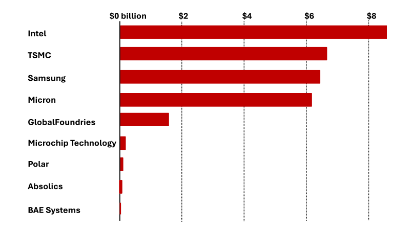
Exhibit II. Total Chips Act incentive grants awarded since December 2023, by receiving company. (source: Wall Street Journal)
The consortium brings together domestic and overseas company partners in the areas of synthesis of specialty chemicals and materials, development and optimization of thin film vapor and liquid phase deposition intensification techniques, and design, construction, and deployment of processing tools and systems. By locating the headquarters and primary operations of the consortium in a specific state, the state would also benefit from the consortium concrete plans to in-source additional specialty chemical and equipment companies and high-tech jobs from overseas to complete the establishment of the critical mass necessary for technology development and commercialization.
The vision and mission of the consortium are:
Vision: To establish a reliable and dependable specialty semiconductor chemical and material vendor consortium, one that would support the strategic interests and economic competitiveness of the U.S. Federal government, individual states, as well as American computer chip corporations, in integrated circuitry (IC) innovation and manufacturing. By creating a pioneering domestic specialty chemical and material supplier resource, as well as attracting and anchoring foreign vendors, this initiative will not only supply current domestic industry packaging needs, but also contribute innovations that would shield the U.S. and its IC industry from future risks related to dependence on foreign suppliers, particularly outfits that could be averse to US interests. To this end, this innovation and commercialization hub is intended as a resource for R&D and manufacturing of novel chemical, material, process, and equipment solutions for nanoscale IC applications.
Mission: To design, demonstrate, and implement novel semiconductor specialty chemicals and materials and process intensification techniques for thin film solutions for incorporation in on-chip and off-chip (packaging) applications. The goal is to enable cohesive, streamlined, and cost-effective uniformity in the fabrication of future generations of on-chip and off-chip heterogeneous IC systems with identical or complementary sets of elemental building blocks and manufacturing protocols. To this end, the intellectual property (IP) developed under this initiative will not only provide enabling significant advancements in IC technologies but will also produce effective technological barriers to overseas competition. A concurrent mission is to create a fully integrated educational and training pipeline of a well-qualified, highly skilled, and tech-savvy workforce for all levels of the IC industry ecosystem.
Learn More About Kalark Nanostructure Sciences.