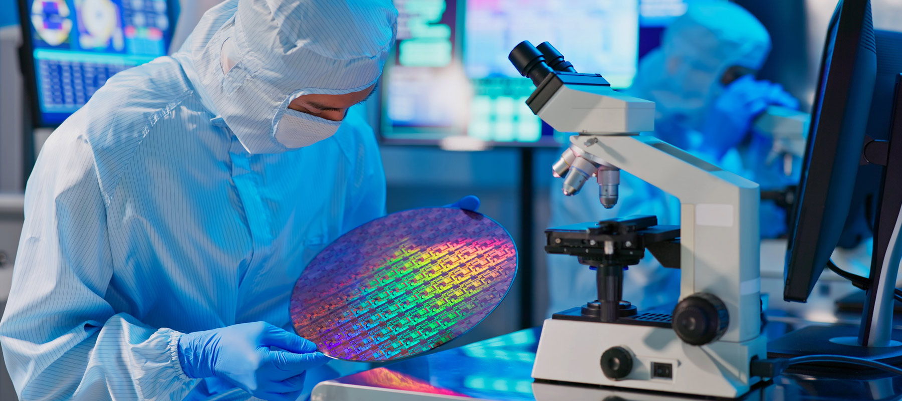
Developing Innovative Solutions for the IC Industry
Kalark Nanostructure Sciences was founded in 2023 as a high-tech U.S. corporation devoted to:
- Performing R&D and commercialization of advanced chemistry, process, and material solutions for the manufacturing of advanced IC devises and system. Our objective is to become a U.S. leader in the discovery, development and commercialization of chemical sources, process expertise, and nanoscale material systems for the IC industry. Our approach provides complete chemical-process-material solutions that bridge chemistry, physics, biology, and materials science and engineering within a technically creative and financially leveraged R&D and manufacturing innovation loop.
- Establishing mutually beneficial partnerships and joint ventures with national and international corporate partners, KNS aims to leverage collective knowledge base, funding, infrastructure, and business relations to create a reliable and dependable U.S.-based semiconductor vendor base. Such a base would not only supply current domestic industry needs, but also contribute innovations that would shield the U.S. semiconductor industry from future liabilities related to dependence on foreign suppliers, particularly outfits that could be averse to US interests.
- Making comprehensive investments and acquisitions to attract and relocate overseas suppliers in the U.S., by offering investments, management and marketing expertise, and enabling new product innovation and greater financial resources.
Our objective is to design, demonstrate, and implement novel semiconductor specialty chemicals and materials and process intensification techniques for thin film solutions for heterogeneous integration in on-chip and off-chip (packaging) applications for high-performance computing (HPC). The goal is to enable coherent, streamlined, and cost-effective uniformity in the fabrication of future generations of on-chip and off-chip heterogeneous IC systems with identical or complementary sets of elemental building blocks and manufacturing protocols. To this end, the intellectual property developed by Kalark will not only provide enabling significant advancements in IC technologies but will also produce effective technological barriers to overseas competition.
- Chemically engineered specialty chemicals. These chemistries would fall under two classes: (i) precursors that are customized to achieve target thin film properties for existing on-chip and off-chip materials under simpler and more straightforward deposition or etching protocols than currently available in the IC industry; and (ii) precursors that are designed to form heterogeneously integrated thin film structures for the plethora of new semiconductor materials, as predicted by the Semiconductor Research Corporation (SRC) Microelectronics and Advanced Packaging Technologies Roadmap (MAPT) and the UCLA Chips and SEMI USA Manufacturing Roadmap for Heterogeneous Integration and Electronics Packaging (MRHIEP). These precursors would also include synthesis of specialty chemicals and materials for existing and novel solid, liquid, and gaseous metal-organic, organo-metallic, and organic chemical sources, including air-sensitive and flammable precursors, in leakage and spill-proof customized vessels that are tailored to target specifications.
- Optimized thin film deposition recipes and equipment. These include chemical vapor deposition (CVD), pulsed CVD, atomic layer deposition (ALD), molecular layer deposition (MLD), self-assembled monolayer (SAM) deposition, Click deposition, atomic layer etching (ALE), and spin-on technologies to enable high precision and tight control in the formation of target thin films and structures. The intent is to demonstrate optimized equipment architecture and process recipes for thin films for incorporation in prevailing semiconductor process flows for on-chip and off-chip heterogeneous integration.
- Intellectual property (IP) portfolios and licenses to enable significant advancements in IC technologies and place effective technological barriers to overseas competition.
- Proprietary proof of concept work and joint demonstration projects (deposition and/or etching) for chemical synthesis, process development, and equipment optimization for emerging on-chip and off-chip technologies with the primary chain of chip manufacturers in an integrated on-site “demo” laboratory. These projects include the identification and implementation of high-risk, high pay-off, “skunkworks” type projects for chemical synthesis, thin film deposition, and equipment optimization quickly, efficiently, and effectively, either based on requests from the primary chain of chip manufacturers or as proposed by the alliance internal R&D teams in response to customer needs and requirements.
- Establishment of a reliable and dependable U.S.-based specialty chemical and material vendor supply capability for synthesis and packaging of existing and novel solid, liquid, and gaseous metal-organic, organo-metallic, and organic chemical sources, including air-sensitive and flammable precursors, in leakage and spill-proof customized vessels that are tailored to target specifications.
- Partnerships with high-schools, community colleges, four-year degree institutions, and public-private foundations to establish new curricula and degree granting programs in pertinent fields of computer chip R&D and manufacturing. The overall objective is to create a fully integrated educational and training foundation to build a pipeline of a well-trained, highly skilled, and tech-savvy workforce for the secondary chain of computer chip industrial companies (chemical and materials producers, component suppliers, OEMs, packaging and testing concerns). This initiative would include working with pertinent Federal and state agencies to provide scholarships, fellowships, and career awards to attract and retain qualified individuals at all levels of the educational food chain, from high-school level through two- and four-year college programs.
Contact Us to learn how we can help you.